-40%
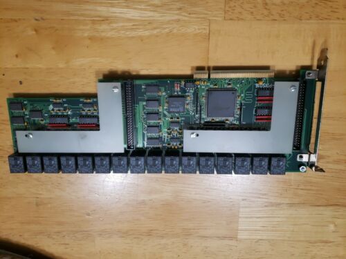
National Instruments PCI-6024E 16-Channel DAQ Data Acquisition Board
$ 170.27
- Description
- Size Guide
Description
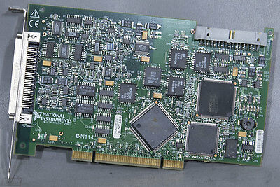
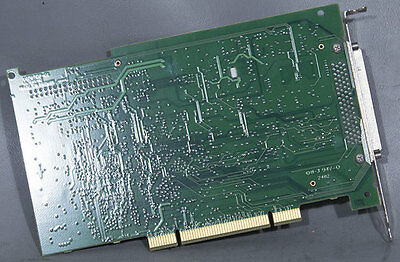
National Instruments PCI-6024E 16-Channel DAQ Data Acqusition BoardComes with what you see in the pictures. If you don't see it, you probably won't get it.
Specifications are from Natioand may vary slightly due to upgrades, options, or revisions this unit may or may not have.
This board is guaranteed to work.
The Unit's Serial Number Tag Reads:
Model Number:
PCI-6024E
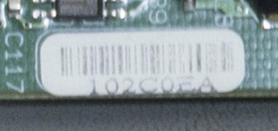
Serial Number:
102C0EA
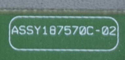
Part Number:
187570C-02
CE Marked:
Yes
Key Features:
16 Channel
200 kS/s Sampling Rate
12-Bit
2 AO
8 DIO
2 24-Bit Counters
Description:
The NI PCI-6024E is a low-cost DAQ board that uses E Series technology to deliver high-performance, reliable DAQ capabilities in a wide range of applications. You get up to 200 kS/s sampling and 12-bit resolution on 16 single-ended analog inputs. Depending on your type of hard drive, the PCI-6024E can stream to disk at rates up to 200 kS/s.
Using NI hardware and driver software options, you have flexible OS, application development environment, and application software choices.
Analog Input Specifications:
Input Characteristics:
Number of Channels:
16 single-ended or 8 differential (software-selectable per channel)
Type of A/D Converter (ADC):
Successive approximation
Resolution:
12 bits, 1 in 4,096
Max. Sampling Rate:
200 kS/s guaranteed
Input Signal Ranges (Bipolar Only):
20 V Range:
±10 V (Bipolar)
10 V Range:
±5 V (Bipolar)
1 V Range:
±500 mV (Bipolar)
100 mV:
±50 mV (Bipolar)
Input Coupling:
DC
Max Working Voltage (Signal + Common Mode):
Each input should remain within ±11 V of ground
Overvoltage Protection:
Signal:
Powered On:
Powered Off:
AI <0..15>
±42
±35
AI SENSE
±40
±25
FIFO Buffer Size:
512 S
DMA (PCI/PXI Only):
Channels:
1
Data Sources/Destinations:
Analog input, analog output, counter/timer 0, or counter/timer 1
DMA Modes
1
:
Scatter-gather (single transfer, demand transfer)
Configuration Memory Size:
512 words (1 word = 8 bits)
Nominal Range (V):
Absolute Accuracy:
Relative Accuracy
Resolution (mV):
Positive Full
Scale:
Negative
Full
Scale:
% of Reading:
Offset
(mV):
Noise + Quantization (mV):
Temp.
Drift
(%/°C)
Absolute
Accuracy at
Full Scale
(mV):
Single
Pt.:
Averaged:
24 Hours:
1 Year:
Single Pt.:
Averaged:
10
-10
0.0872
0.0914
6.38
3.91
0.975
0.0010
16.504
5.89
1.28
5
-5
0.0272
0.0314
3.20
1.95
0.488
0.0005
5.263
2.95
0.642
0.5
-0.5
0.0872
0.0914
0.340
0.195
0.049
0.0010
0.846
0.295
0.064
0.05
-0.05
0.0872
0.0914
0.054
0.063
0.006
0.0010
0.106
0.073
0.008
Note:
Accuracies are valid for measurements following an internal E Series calibration. Averaged numbers assume dithering and averaging of 100 single-channel readings. Measurement accuracies are listed for operational temperatures within ±1°C of internal calibration temperature and ±10°C of external or factory-calibration temperature. NI recommends a one-year calibration interval. The Absolute Accuracy at Full Scale calculations were performed for a maximum range input voltage (for example, 10 V for the ±10 V range)the ±10 V range) after one year, assuming 100 points of averaged data.
Transfer Characteristics:
Relative Accuracy:
Dithered:
±0.5 LSB typ
Undithered:
±1.5 LSB max
Differential Nonlinearity (DNL):
±0.5 LSB typ, ±1.0 LSB max
No Missing Codes:
12 bits, guaranteed
Offset Error:
Pregain Error After Calibration:
±12 µV max
Pregain Error Before Calibration:
±28 mV max
Postgain Error After Calibration:
±0.5 mV max
Postgain Error Before Calibration:
±100 mV max
Gain Error (Relative to Calibration Reference):
After Calibration (gain = 1):
±0.02% of reading max
Before Calibration:
±2.75% of reading max
Gain ≠1 with Gain Error Adjusted to 0 at Gain = 1:
±0.05% of reading max
Amplifier Characteristics:
Input Impedance:
Normal Powered On:
100 GΩ in parallel with 100 pF
Powered Off:
4.7 kΩ
Overload:
4.7 kΩ
Input Bias Current:
±200 pA
Input Offset Current:
±100 pA
Common-Mode Rejection Ratio (CMRR), DC to 60 Hz:
Range 10 to 20 mV:
85 dB
Range 100 mV to 1 V:
90 dB
Dynamic Characteristics:
Bandwidth:
Small Signal (-3 dB):
500 kHz
Large Signal (1% THD):
225 kHz
Settling Time for Full-Scale Step:
5 µs typ. to ±1.0 LSB accuracy
1
System Noise (LSB
rms
, not including quantization):
Device:
Range:
Dither Off:
Dither On:
NI 6023E, PCI-6024E, 6025E:
1 to 20 V
0.1
0.6
100 mV
0.7
0.8
Crosstalk:
-60 dB, DC to 100 kHz
Stability:
Recommended Warm-Up Time:
15 minutes
Offset Temperature Coefficient:
Pregain:
±15 µV/°C
Postgain:
±240 µV/°C
Cain Temperature Coefficient:
±25 ppm/°C
Notes:
1:
DMA is not available on the NI DAQCard-6024E.
Analog Output Specifications:
Output Characteristics:
Number of Channels:
2 voltage
Resolution:
12-bit, 1 in 4,096
Max Update Rate:
DMA
1
:
10 kHz, system dependent
Interrupts:
1 kHz, system dependent
Typa of D/A Converter (DAC):
Double-buffered, multiplying
FIFO Buffer Size:
None
Data Transfers:
DMA
1
, interrupts, programmed I/O
Accuracy Information:
Nominal Range (V):
Absolute Accuracy:
Absolute
Accuracy
at Full
Scale (mV):
Positive
Full Scale:
Negative
Full Scale:
% of Reading:
Offset
(mV):
Temp. Drift
(%/°C):
24 Hours:
90 Days:
1 Year:
10
-10
0.0177
0.0197
0.0219
5.93
0.0005
8.127
Note:
Accuracies are valid for measurements following an internal E Series Calibration. Averaged numbers assume dithering and averaging of 100 single-channel readings. Measurement accuracies are listed for operational temperatures within ±1°C of internal calibration temperature and ±10°C of external or factory-calibration temperature. NI recommends a one-year calibration interval. The Absolute Accuracy at Full Scale calculations were performed for a maximum range input voltage (for example, 10 V for the ±10 V range) after one year, assuming 100 points of averaged data.
Transfer Characteristics:
Relative Accuracy or Integral Nonlinearity (INL) - After Calibration:
±0.3 LSB typ, ±0.5 LSB max
Relative Accuracy or Integral Nonlinearity (INL) - Before Calibration:
±4 LSB max
DNL:
After Calibration:
±0.3 LSB typ, ±1.0 LSB max
Before Calibration:
±3 LSB
Monontonicity:
12 bits, guaranteed after calibration
Offset Error:
After Calibration:
±1.0 mV max
Before Calibration:
±200 mV max
Gain Error (Relative to Internal Reference):
After Calibration:
±0.01% of output max
Before Calibration:
±0.75% of output max
Voltage Output:
Range:
±10 mV
Output Coupling:
DC
Output Impedance:
0.1 Ω max
Current Drive:
±5 mA max
Protection:
Short-circuit to ground
Power-On State (Steady State):
±200 mV
Initial Power-Up Glitch:
Magnitude:
±1.1 V
Duration:
2.0 ms
Power Reset Glitch:
Magnitude:
±2.2 V
Duration:
4.2 µs
Dynamic Characteristics:
Settling Time for Full-Scale Step:
10 µs to ±0.5 LSB accuracy
Slew Rate:
10 V/µs
Noise:
200 µ/V
rms
, DC to 1 MHz
Midscale Transition Glitch:
Magnitude:
±42 mV
Duration:
2.0 µs
Stability:
Offset Temperature Coefficient:
±50 µV/°C
Gain Temperature Coefficient:
±25 ppm/°C
Digital I/O:
Number of Channels:
8 input/output
Compatibility:
5 V TTL
Digital Logic Level on P0.<0..7>:
Level:
Min.:
Max.:
Input Low Voltage:
0 V
0.8 V
Input High Voltage:
2.0 V
5.0 V
Input Low Current:
(V
in
= 0 V)
-
-320 µA
Input High Current:
(V
in
= 5 V)
-
10 µA
Output Low Voltage:
(I
OL
= 24 mA)
-
-75 µA
Output High Voltage (I
OH
= -13 mA)
4.35 V
-
Power-On State:
Input (high-impedance), 50 kΩ pull-up to +5 VDC
Data Transfers:
Programmed I/O
Handshaking:
2-wire
Power-On State:
P1.<0..7>:
Input (high-impedance), 100 kΩ pull-up to +5 VDC
P2.<0..7>:
Input (high-impedance), 100 kΩ pull-up to +5 VDC
P3.<0..7>:
Input (high-impedance), 100 kΩ pull-up to +5 VDC
Data Transfers:
Interrupts, programmed I/O
Timing I/O:
Number of Channels:
2 up/down, counters/timers, 1 frequency scaler
Resolution:
Counter/Timers:
24 bits
Frequency Scalers:
4 bits
Compatibility:
5 V/TTL
Base Clocks Available:
Counters/Timers:
20 MHz, 100 kHz
Frequency Scalers:
10 MHz, 100 kHz
Base Clock Accuracy:
±0.01%
Max. Source Frequency Up/Down Counter/Timers:
20 MHz
Min. Source Pulse Duration:
10 ns in edge-detect mode
Min. Gate Pulse Duration:
10 ns in edge-detect mode
Data Transfers:
DMA
1
, interrupts, programmed I/O
DMA Modes
1
:
Scatter-gather (single transfer, demand transfer)
Triggers Specifications:
Digital Trigger:
Purpose:
Analog Input:
Start, reference, and pause trigger, sample clock
Analog Output:
Start and pause trigger, sample clock
Counters/Timers:
Source, gate
External Sources:
PFI<0..9>, RTSI<0..6>
Compatibility:
5 V TTL
Response:
Rising or falling edge
Pulse Width:
10 ns min.
RTSI (PCI and PXI Only) Specifications:
Trigger Lines:
7
Calibration Specifications:
Recommended Warm-up Time:
15 minutes
Interval:
1 year
External Calibration Reference:
Between 6 and 10 V
Onboard Calibration Reference:
Level:
5.00 V (±3.5 mV), actual value stored in EEPROM
Temperature Coefficient:
±5 ppm/°C max
Long-term Stability:
±15 ppm/√1,000 h
Power Reuirement Specifications:
+5 VDC (±5%):
0.7 A
Power Available at I/O Connector:
+4.65 to +5.25 VDC at 1 A
Physical Specifications:
Dimensions:
17.5 cm x 10.7 cm (6.9" x 4.2")
Weight:
115 g (4.1 oz)
I/O Connector:
68-pin male SCSI-II type
Maximum Working Voltage Specifications:
Channel-to-Earth:
11 V, Installation Category I
Channel-to-Channel:
11 V, Installation Category I
Environmental Specifications:
Operating Temperature:
0 to 55°C
Storage Temperature:
-20 to 70°C
Relative Humidity:
10 to 90% noncondensing
Maximum Altitude:
2,000 m
Pollution Degree (Indoor Use Only):
2
Safety Compliance Specifications:
IEC 61010-1, EN 61010-1
UL 61010-1
CAN/CSA-C22.2 No. 61010-1
Electromagnetic Compatibility Specifications:
Emissions:
EN 55011 Class A at 10 m. FCC Part 15A above 1 GHz.
Immunity:
EN 61326:1997 A2:2001, Table 1
CE, C-Tick, and FCC Part 15 (Class A) Compliant
CE Compliance Specifications:
Low-Voltage Directive (Safety):
73/23/EEC
Electromagnetic Compatibility Directive (EMC):
89/336/EEC
For Domestic Customers: Packaging, handling, and order processing included in shipping in all domestic shipments as quoted by the shipping calculator. For International Customers there is a .00 minimum for packaging, handling, and order processing. International shipping to be determined by destination.
Prior to shipment I will need to know the following information (filled out on a form that I will send you) for International Customers or Packages/Freight being Forwarded internationally. International customers may also be subject to a freight forwarder form if applicable.:
(1) Are you the end-user of this item?
(2) If you are not the ultimate end-user of the item, please state the ultimate end user's name.
(3) What is the ultimate country destination?
04/14/17
